#statusMessage#
Do you want to start the compare now?
#statusMessage#
Do you want to start the compare now?
With the increasing importance of renewable energies in the wake of climate change, solar energy is moving further into ...
The complexity of military radios and the often harsh weather conditions have a negative impact on the reliability of ra...
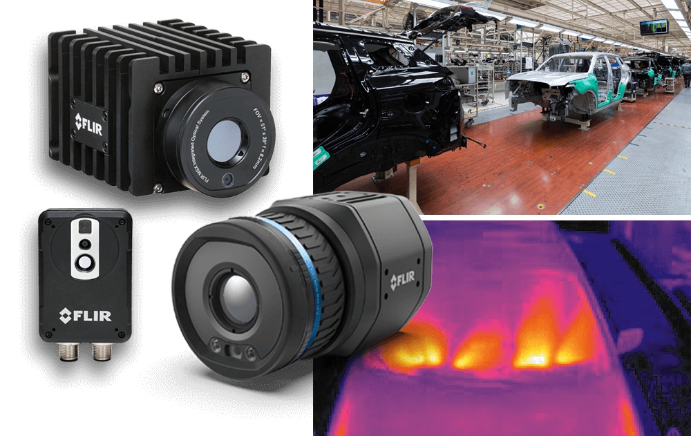
Automation with thermal imaging technology has proven to be a reliable solution for quality control in various industrie...
In diesem exklusiven Whitepaper erfahren Sie, wie Sie mit der richtigen Messtechnik arbeiten: ✔ Sie realisieren ein Test...
Manufacturer number: J2110A
On Request
Since with signals (e.g. the J2100A) in a frequency range from 1 Hz to 5 MHz or more, false signals can be impressed into an Rergel loop, this frequency range is insufficient for some applications. The frequency range can be significantly increased with the J2110A semiconductor voltage impression.
For e.g. For example, a heating control may have a bandwidth below 1 Hz, but bandwidths of 100 MHz and above are decisive for a linear control with an operational amplifier. Broadband semiconductor impressions are necessary for such regulations. These embossing circuits can be used from DC to a frequency that is only determined by the structure (PC board material and layout) and the components used. Bandwidths from DC to 200 MHz can be achieved. Above 50 MHz, the connection between the insertion and the circuit under test can be very critical. It is important that the ripple of the voltage supply of the impressing circuit does not affect the dynamic range or the signal-to-noise ratio of the measurement. The measurement results are often better if the semiconductor embossing circuits such as J2110A are used instead of transformers.
The choice of the correct stamping point in the circuit to be tested is significantly more critical than with a transformer. The impressing circuit has undefined impedances at the impressing point. In order to obtain clear measurement results, one side must offer a higher impedance than the other. In a typical power supply control, the voltage divider for the control loop has a limited voltage range and is therefore the suitable point for an impression, since the output impedance of the power supply is significantly lower than the impedance of the voltage sensor of the control loop.
The output voltage level of the semiconductor impressed circuit has a limit of 10 V or 12 V, which however is not the voltage amplitude of the impressed signal (positive or negative).